
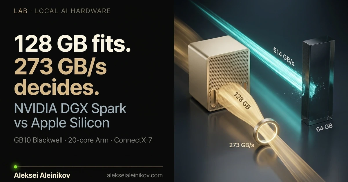
Local AI hardware always forces the same trade-off: discrete GPUs are fast but cramped, while unified-memory workstations are spacious but bandwidth-limited. NVIDIA’s DGX Spark (built on the GB10 Grace Blackwell Superchip) puts 128 GB of coherent unified memory, 1 PetaFLOP of sparse FP4 compute, and a 200 Gb/s ConnectX-7 SmartNIC inside a 150 × 150 mm desktop chassis.
On paper, that sounds like a desktop silver bullet for 70B–200B models. Look at the memory bus, however, and a sharper engineering picture emerges: 273 GB/s of LPDDR5x bandwidth sits next to Apple Silicon configurations delivering 546 to 819 GB/s. Knowing which workload hits which wall is the difference between a well-matched workstation and an expensive bottleneck.
Under the hood: NVIDIA GB10 vs Apple Silicon
The NVIDIA GB10 Grace Blackwell Superchip fuses a 20-core Armv9 CPU (10 Cortex-X925 performance cores + 10 Cortex-A725 efficiency cores) with a Blackwell GPU featuring 5th-generation Tensor Cores over a coherent NVLink-C2C interconnect. Instead of discrete GDDR6X/GDDR7 VRAM wired across PCIe, both processors share 128 GB of LPDDR5x memory across a 256-bit interface running at 8.533 Gbps per pin—yielding 273 GB/s of peak memory bandwidth.
| Specification | NVIDIA DGX Spark (GB10) | Apple M5 Max (40-core GPU) | Apple M4 Max (Mac Studio) | RTX 5090 (Discrete GPU) |
|---|---|---|---|---|
| Memory Capacity | 128 GB unified (64 GB OEM tier) | 64 GB tested (48–128 GB options) | Up to 128 GB unified | 32 GB GDDR7 |
| Memory Bandwidth | 273 GB/s (256-bit LPDDR5x) | 614 GB/s | 546 GB/s | ~1,792 GB/s |
| AI / Tensor Peak | 1,000 TOPS FP4 (with sparsity) | Metal FP16 / BF16 | Metal FP16 / BF16 | ~3,352 TOPS FP4 (sparse) |
| High-Speed Clustering | 200 Gb/s ConnectX-7 RDMA | Thunderbolt 5 (no RDMA NIC) | Thunderbolt 5 (no RDMA NIC) | PCIe / Ethernet host |
| Software Stack | CUDA, TensorRT-LLM, NIM, vLLM | Metal, MLX, llama.cpp | Metal, MLX, llama.cpp | CUDA, TensorRT-LLM, vLLM |
| Chassis & Power | 1.2 kg SFF · 240 W PSU (~140 W TDP) | Laptop / mobile envelope | Compact desktop | Full ATX workstation (575 W GPU) |
| Reference Price | $3,999 launch / $4,699 MSRP (Feb 2026) | $3,599+ base (64 GB BTO) | $3,699 (1 TB) / $4,699 (4 TB) | $1,999 MSRP (GPU only) |
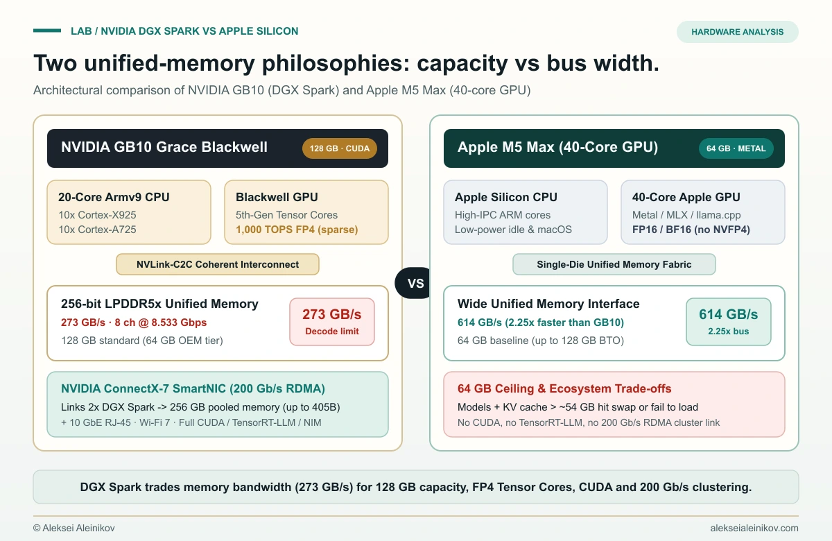
That single architectural choice—256-bit LPDDR5x at 273 GB/s—explains almost everything about DGX Spark’s behavior. NVIDIA kept power (~140 W SoC TDP) and board complexity small enough for a 1.2 kg desk cube while preserving the full CUDA + TensorRT-LLM + NIM ecosystem and ConnectX-7 clustering.
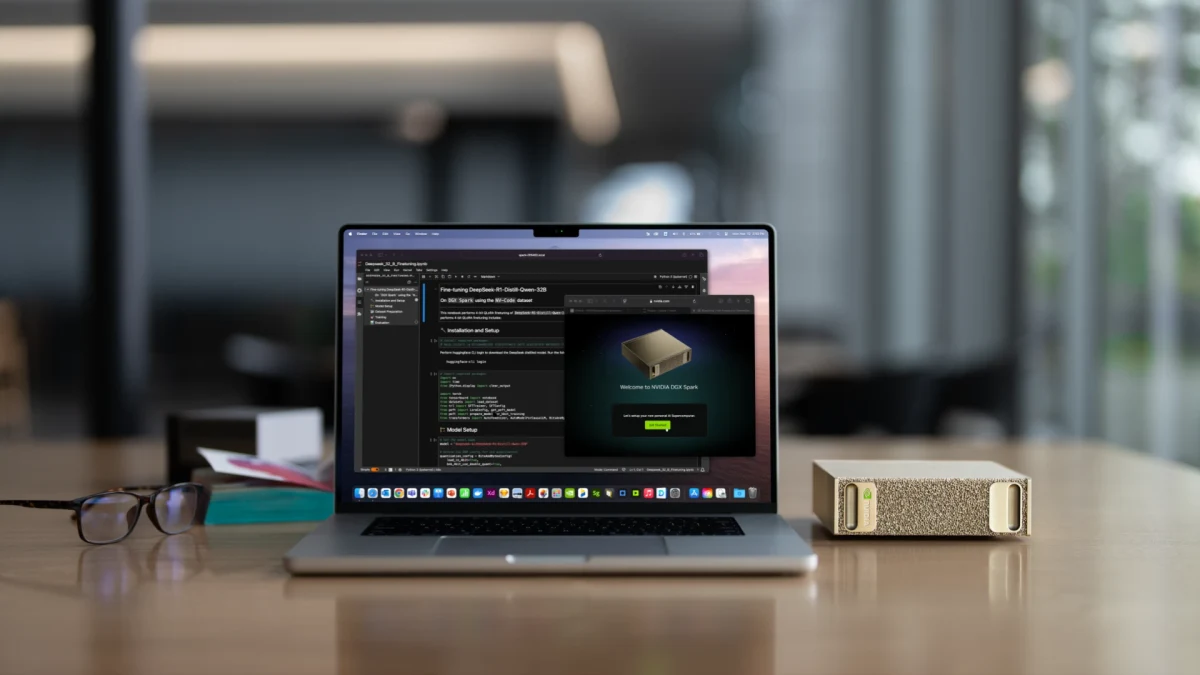
The math of local LLM inference: memory, decode, and prefill
To compare these machines honestly, you have to separate three different physical limits: how much fits in RAM, how fast tokens stream out (decode), and how fast long prompts are digested (prefill).
1. The memory footprint equation
A running LLM consumes unified memory for weights, the Key-Value (KV) cache, and runtime activations:
M_total = M_weights + M_KV(context_length, batch_size) + M_overhead
M_weights ≈ Parameters × (Bits_per_weight / 8)
For a 70B dense model:
- At Q4_K_M (~4.6–4.8 bits/weight effective), weights alone take ~40.5 GB. Add a 32k context KV cache and runtime buffers, and you are around 48–52 GB—barely inside a 64 GB machine (after macOS/Linux overhead), and completely impossible on a 32 GB GPU.
- At FP8 (~8 bits/weight), weights take ~70 GB. A 64 GB machine cannot load it at all; DGX Spark’s 128 GB holds it comfortably with room for long context or LoRA adapters.
2. Why 1 PFLOP does not fix single-user decode
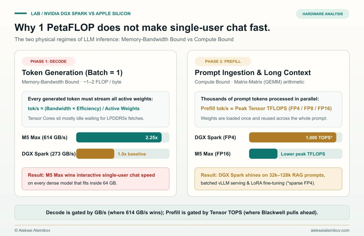
During single-stream generation (batch size = 1), arithmetic intensity is roughly 1 to 2 FLOPs per byte loaded from memory. The GPU cannot compute the next token until it streams all active weights from LPDDR5x into SRAM:
Decode Ceiling (tok/s) = (Memory Bandwidth × η) / Active_Weight_BytesHere, η (bandwidth utilization efficiency) is typically 0.60 to 0.85 depending on kernel efficiency, quantization packing, and KV-cache reads.
Plug in a ~40.5 GB Q4_K_M 70B model:
- DGX Spark (273 GB/s): Idealized ceiling
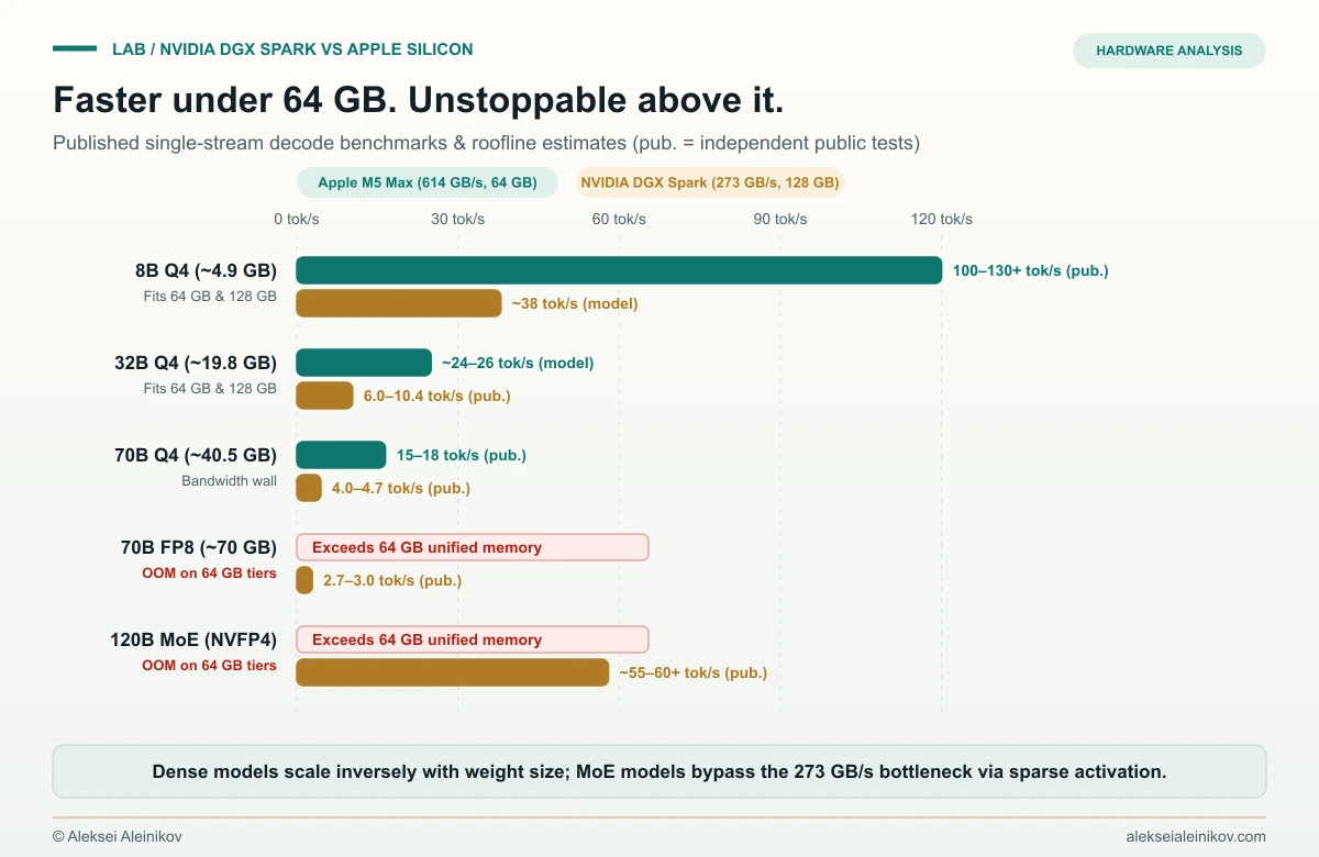
273 / 40.5 = 6.74 tok/s. With realisticη ≈ 0.65, you land at ~4.4 tok/s—matching published independentllama.cppbenchmarks of 4.0 to 4.7 tok/s (and 2.7–3.0 tok/s in FP8vLLM). - Apple M5 Max (614 GB/s): Idealized ceiling
614 / 40.5 = 15.16 tok/s. Withη ≈ 0.78, you land near ~11.8 tok/s—more than 2.5× faster interactive reading speed, provided the model and context stay under the ~54–56 GB usable macOS memory ceiling.
3. Where Blackwell’s 1,000 TOPS actually shines: prefill & MoE
During prefill (ingesting a 32k-token RAG prompt, codebase, or PDF), all prompt tokens are processed in parallel as dense matrix-matrix multiplications (GEMM). Arithmetic intensity shoots up, and the workload becomes compute-bound.
Here, Blackwell’s 5th-generation Tensor Cores (1,000 AI TOPS at sparse FP4) completely flip the table: published DGX Spark tests report ~800+ tok/s prefill on 70B models—far faster than consumer unified-memory laptops.
DGX Spark is not a single-stream dense-70B chat box. It is a high-capacity prefill, fine-tuning, and Mixture-of-Experts (MoE) workstation—and a building block for 256 GB two-node clusters.
Similarly, Mixture-of-Experts (MoE) models (such as 120B-class sparse architectures where only ~10–12B parameters activate per token) break the decode bottleneck. The full 120B weights sit comfortably inside Spark’s 128 GB memory, yet each token only streams the active experts—pushing DGX Spark into the 50–60+ tok/s range while a 64 GB machine cannot even load the weights.
Published benchmarks vs roofline math
Combining official memory-bandwidth specifications with published independent llama.cpp, MLX, and vLLM benchmarks shows how tightly real-world decode speed tracks the theoretical bandwidth ceiling:
| Model Class | Footprint (Weights) | Apple M5 Max (614 GB/s, 64 GB tier) | Apple M4 Max (546 GB/s) | NVIDIA DGX Spark (273 GB/s, 128 GB) |
|---|---|---|---|---|
| 8B Dense (Q4_K_M) | ~4.9 GB | 100–130+ tok/s (published MLX/llama.cpp) | 115–130 tok/s (published) | ~35–38 tok/s (roofline estimate, η ≈ 0.65) |
| 32B Dense (Q4_K_M) | ~19.8 GB | ~24–26 tok/s (roofline estimate, η ≈ 0.78) | ~21–23 tok/s (roofline estimate) | 6.0–10.4 tok/s (published Ollama/vLLM) |
| 70B Dense (Q4_K_M) | ~40.5 GB | 15–18 tok/s (published Q4/Q5) | 13–15.5 tok/s (published) | 4.0–4.7 tok/s (published llama.cpp) |
| 70B Dense (FP8) | ~70 GB | OOM (>64 GB ceiling) | Fits on 128 GB BTO tier | 2.7–3.0 tok/s (published vLLM; ~800+ tok/s prefill) |
| 120B MoE (NVFP4 / Q4) | ~65–75 GB | OOM (>64 GB ceiling) | Fits on 128 GB BTO tier | ~55–60+ tok/s (published community tests) |
If you want to understand how quantization levels like Q4_K_M, FP8, and NVFP4 change these exact memory footprints without destroying accuracy, see the companion breakdown on running large models on constrained hardware:
Quantization Explained: Running 70B Models on Consumer Hardware
ConnectX-7 clustering and the CUDA moat
Two features separate DGX Spark from every Apple Silicon Mac on the market, regardless of memory bandwidth:
- 200 Gb/s ConnectX-7 SmartNIC clustering: Each DGX Spark ships with a ConnectX-7 port capable of 200 Gb/s RDMA over QSFP/DAC cables. Linking two units pools 256 GB of unified memory, pushing local inference capacity up to 405B-class quantized models. Apple’s Thunderbolt 5 cannot match true RDMA NIC fabric for distributed NCCL/tensor-parallel workloads.
- Native CUDA, TensorRT-LLM, and NIM parity: If your production target runs vLLM, TensorRT-LLM, CUDA kernels, or NVIDIA NIM containers, developing and debugging on an Arm + Blackwell Linux box avoids the Metal-to-CUDA translation gap entirely. For serving workflows, choosing between vLLM and Ollama matters far more once continuous batching enters the picture—under concurrent requests, DGX Spark’s aggregate throughput scales much better than single-stream latency suggests.
Price reality and TCO: $3,999 launch vs $4,699 official MSRP
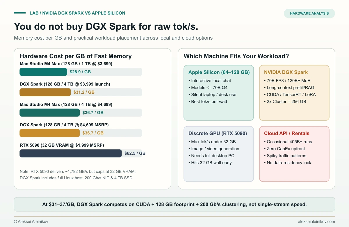
NVIDIA launched the 128 GB / 4 TB DGX Spark Founders Edition at $3,999 MSRP (~$31.24 per GB of unified memory). In February 2026, citing global LPDDR5x memory supply constraints, NVIDIA officially raised its store MSRP to $4,699, while some regional retail and partner listings have climbed as high as $6,950.
At $4,699, DGX Spark sits at $36.71 per GB—almost the exact price of a Mac Studio M4 Max with 128 GB unified memory and 4 TB SSD ($4,699), which delivers 546 GB/s (2× the memory bandwidth of Spark) in exchange for losing CUDA, FP4 Tensor Cores, and ConnectX-7. Meanwhile, an RTX 5090 ($1,999 MSRP) delivers ~1,792 GB/s for unmatched speed under 32 GB, but costs $62.47 per GB of VRAM before you even buy a CPU, motherboard, PSU, or 128 GB of system RAM.
The bottom line: who should actually buy DGX Spark?
- Choose DGX Spark (128 GB) if you need 70B+ / 120B+ MoE models, long-context RAG prefill, local QLoRA fine-tuning, native CUDA/TensorRT-LLM/vLLM parity, or plan to link two units via 200 Gb/s ConnectX-7 for a 256 GB desktop cluster.
- Choose Apple Silicon (64–128 GB Mac Studio / MacBook Pro) if your primary goal is fast, quiet, single-user interactive chat on models that fit inside RAM, where 546–819 GB/s delivers roughly double the tokens per second per watt.
- Choose a discrete GPU (RTX 5090) if your models fit under 32 GB VRAM and you want maximum raw decode speed or image/video generation.
- Stay on Cloud APIs if you only touch 400B+ frontier models occasionally and cannot justify $4,000–$5,000+ of upfront CapEx.